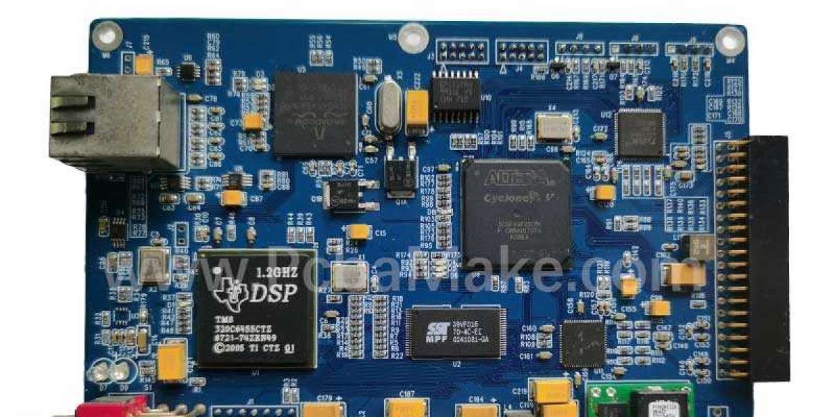
PCB board needs to be inspected during processing, and visual inspection is an important item. Many defects or deficiencies in quality on the PCB can be identified through visual inspection, so effective measures can be taken to improve and continuously improve product quality. When performing visual inspections, some simple optical instruments are sometimes used. For those PCB board manufacturers with imperfect production equipment and testing equipment, visual inspection is more important, and it is essential to improve product quality.
In PCB board processing, visual inspection is mainly used in solder paste printing, component placement and soldering completion; content includes: PCB board manual inspection, glue spot visual inspection, solder joint visual inspection and surface quality visual inspection, etc. The contents of the visual inspection include:
1. Solder paste printing
First check whether the parameter settings of the solder paste printer are correct; whether the height of the solder paste is consistent or shows a "trapezoidal" shape, the edges of the solder paste cannot be rounded or collapsed into a pile, but some are allowed to be pulled up by the steel plate. Peak shape caused by solder paste. If the solder paste is unevenly distributed, check the solder paste on the squeegee for insufficient or uneven distribution, and check the printed steel plate and other parameters. Finally, check under the microscope whether the solder paste is bright after printing.
2. Component placement
Before inserting the components on the first quick turn PCB with solder paste, visually check whether the rack is placed, whether the components that need to be used meet the production requirements, and whether the picking position of the equipment is accurate. After completing the first PCB, inspect each component carefully by visual inspection to see if they are all correctly placed and gently pressed in the center of the solder paste. If you see a slight depression in the solder paste pressed by the component in the microscope, it means that the component is placed correctly. Also visually inspect all the components on the BOM list to see if they are consistent with the components on the PCB; more importantly, visually inspect those components that are sensitive to the positive and negative electrodes, such as diodes, tantalum electrolytic capacitors, and ICs. To see if they are placed in the correct direction.


